There are way too many different types of semiconductor (IC or transistor) packages.
For example, SOP, QFN and BGA are some of the package names, but it is very difficult to understand which package represents which shape.
Therefore, in this article, we have summarized the types and characteristics of each package in an easy-to-understand manner using diagrams. We hope you will find it helpful.
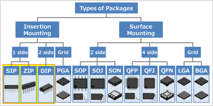
List of IC Package Types
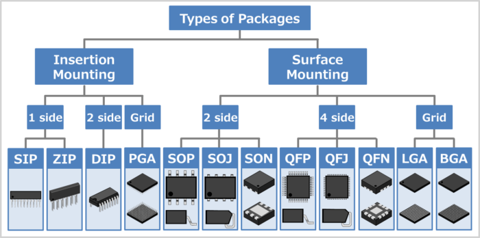
The figure above shows the classification of packages. Packages can be broadly classified according to the following aspects.
- Difference in mounting method
- Whether the mounting method is "insertion mounting" or "surface mounting".
- Difference in terminals
- Whether the terminals (leads, etc.) are "from 1 side", "from 2 sides", "from 4 sides", or "in a grid".
Now, we will explain each package in detail.
Related article
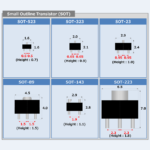
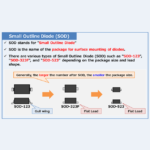
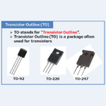
In addition to the packages shown in the above figure, SOT (SOT-23, etc.), SOD (SOD-323, etc.), and TO (TO-220, etc.) are also available.
SOT (SOT-23, etc.), SOD (SOD-323, etc.),and TO (TO-220, etc.) are explained in detail in the article below. If you are interested, please click the link below.
-

What is Small Outline Transistor (SOT)?
続きを見る
-
What is Small Outline Diode (SOD)?
続きを見る
-
What is Transistor Outline (TO)?
続きを見る
Types of IC Packages for Insertion Mounting
There are SIP, DIP, ZIP, and LGA packages for insertion mounting.
The main points of SIP, DIP, and ZIP are shown below (LGA will be explained in detail later).
Types of IC Packages for Insertion Mounting
- Single In-line Package (SIP)
- The leads come out of one side of the package and the leads are in a single row.
- Zig-zag In-line Package (ZIP)
- The leads come out of one side of the package and the leads zig-zagged out.
- Dual In-line Package (DIP)
- he leads come out of two sides of the package and leads exit downward.
We will now describe each package in turn.
Single In-line Package (SIP)
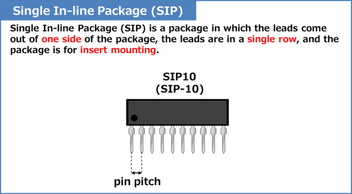
SIP stands for "Single In-line Package".
Single In-line Package (SIP) is a package in which the leads come out of one side of the package, the leads are in a single row, and the package is for insert mounting. SIP is sometimes described as SIL.
Single In-line Package (SIP) has 2 to 23 pins.
The number after SIP indicates the number of pins. For example, SIP10 means a 10-pin SIP.
Single In-line Package (SIP) has the leads on the long side of the package and is mounted upright on the PCB. Since the package can be mounted upright, the mounting density of the PCB can be increased compared to the Dual In-line Package (DIP).
SIP is used not only in IC but also in network resistors and transistor arrays that require heat dissipation.
There are various types of SIP, such as HSIP and P-SIP.
Related article
The following article explains the "Single In-line Package (SIP)" in detail. If you are interested, please check it out from the link below. 続きを見る
What is Single In-line Package (SIP)?
Zig-zag In-line Package (ZIP)
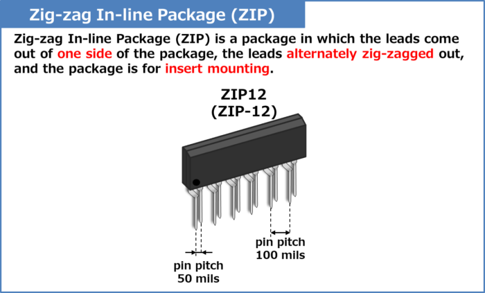
ZIP stands for "Zig-zag In-line Package".
Zig-zag In-line Package (ZIP) is a package in which the leads come out of one side of the package, the leads alternately zig-zagged out, and the package is for insert mounting.
Zig-zag In-line Package (ZIP) has 12 to 40 pins.
The number after ZIP indicates the number of pins. For example, ZIP12 means a 12-pin ZIP.
It is the same as Single In-line Package (SIP) in that the leads come out of one side of the package. However, the Zig-zag In-line Package (ZIP) has a zigzag shape of the lead, which allows the pin pitch to be shortened, thus shortening the long side.
The pin pitch of the ZIP (Zig-zag In-line Package) is 50 mils when the package face is viewed from the front, but 100 mils when it is inserted into the PCB.
There are various types of ZIP, such as SZIP and HZIP.
Related article
The following article explains the "Zig-zag In-line Package (ZIP)" in detail. If you are interested, please check it out from the link below. 続きを見る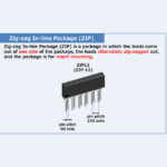
What is Zig-zag In-line Package (ZIP)?
Dual In-line Package (DIP)
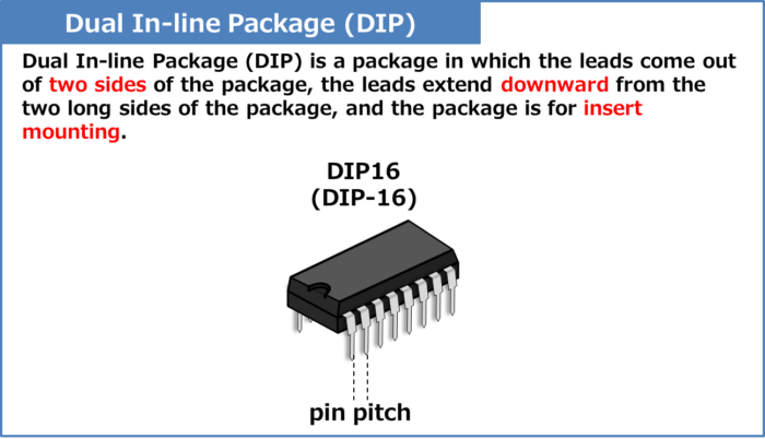
DIP stands for "Dual In-line Package".
Dual In-line Package (DIP) is a package in which the leads come out of two sides of the package, the leads extend downward from the two long sides of the package, and the package is for insert mounting.
Dual In-line Package (DIP) has 6 to 64 pins.
The number after DIP indicates the number of pins. For example, DIP16 means a 16-pin DIP.
Dual In-line Package (DIP) is available in a variety of pin pitch distances. The normal pin pitch is 100 mils (2.54mm), but there are some with a pin pitch of 70 mils (1.778mm). Package widths include 600 mils (15.2mm), 400 mils (10.16mm), and 300 mils (7.62mm).
There are various types of DIP, such as SDIP and HSDIP.
Related article
The following article explains the "Dual In-line Package (DIP)" in detail. If you are interested, please check it out from the link below. 続きを見る
What is Dual In-line Package (DIP)?
Types of IC Packages for Surface Mounting
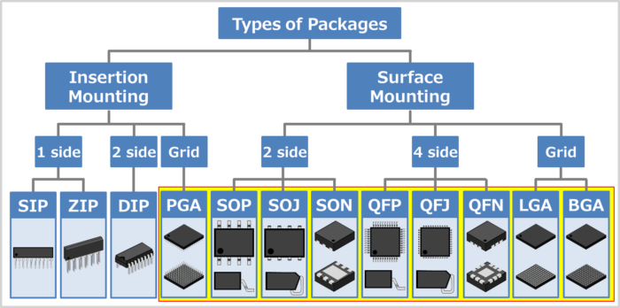
The following types of packages are available for insertion mounting.
Types of IC Packages for Surface Mounting
- Packages with leads coming out of two sides of the package
- SOP, SOJ, SON, etc.
- Packages with leads coming out of four sides of the package
- QFP, QFJ, QFN, etc.
- Packages with terminals arranged in a grid pattern from the bottom of the package
- PGA, LGA, BGA, etc. (Only PGA is Insertion Mounting).
Packages with leads coming out of two sides of the package are often marked with SO. SO stands for "Small Outline". The shape of the lead is determined by the letter that comes after the SO, as shown below.
SO Package Lead Shape
- SOP: Gull-wing (L-shaped) type
- SOJ: J-lead type
- SON: Non-leaded (no lead) type
- SOI: I-lead type
- SOF: Flat lead type
Packages with leads coming out of four sides of the package are often marked with QF. QF stands for "Quad Flat". The shape of the lead is determined by the letter that comes after the QF, as shown below.
QF Package Lead Shape
- QFP: Gull-wing (L-shaped) type
- QFJ: J-lead type
- QFN: Non-leaded (no lead) type
- QFI: I-lead type
- QFF: Flat lead type
Packages with terminals arranged in a grid pattern from the bottom of the package are often marked with GA. GA stands for "Grid Array". The shape of the lead is determined by the letter that comes before the GA, as shown below.
QF Package Lead Shape
- PGA: Pin type
- LGA: Land type
- BGA: Solder Balls type
Now, we will explain each package in detail.
Small Outline Package (SOP)
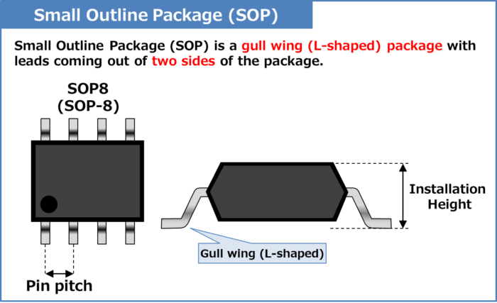
SOP stands for "Small Outline Package".
Small Outline Package (SOP) is a gull wing (L-shaped) package with leads coming out of two sides of the package. The pin pitch of the SOP (Small Outline Package) is 50 mils (1.27mm).
The number after SOP indicates the number of pins. For example, SOP8 means a 8-pin SOP.
In packages with a pin pitch of 1.27mm, those with a JEITA standard are SOP (Small Outline Package) and those with a JEDEC standard are SOIC (Small Outline Integrated Circuit). Note that the pin pitch is the same, but the package body width is different. SOIC is also sometimes referred to as "SOL (Small Outline L-leaded package)" or "SO".
In addition, those with gull wing (L-shaped) leads coming out of the four sides of the package are called Quad Flat Package (QFP).
There are various types of SOP, such as SSOP and MSOP.
Related article
The following article explains the "Small Outline Package (SOP)" in detail. If you are interested, please check it out from the link below. 続きを見る
What is Small Outline Package (SOP)?
Small Outline J-leaded package (SOJ)
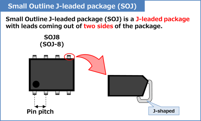
SOJ stands for "Small Outline J-leaded package".
Small Outline J-leaded package (SOJ) is a J-leaded package with leads coming out of two sides of the package. The pin pitch of the Small Outline J-leaded package (SOJ) is 50 mils (1.27mm).
The number after SOJ indicates the number of pins. For example, SOJ8 means a 8-pin SOJ.
Compared to Small Outline Package (SOP), which has a gull wing (L-shaped) lead shape, Small Outline J-leaded package (SOJ), which has a J-shaped lead shape, has the advantage of less lead deformation.
In addition, those with J-shaped leads coming out of the four sides of the package are called Quad Flat J-leaded package (QFJ).
There are various types of SOJ, such as P-SOJ and C-SOJ.
Related article
The following article explains the "Small Outline J-leaded package (SOJ)" in detail. If you are interested, please check it out from the link below. 続きを見る
What is Small Outline J-leaded package (SOJ)?
Small Outline Non-leaded package (SON)
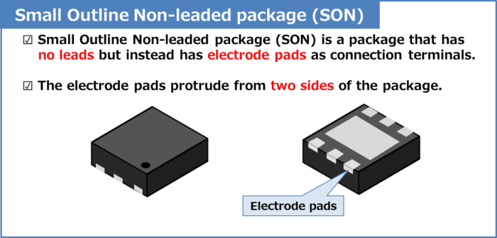
SON stands for "Small Outline Non-leaded package".
Small Outline Non-leaded package (SON) is a package that has no leads but instead has electrode pads as connection terminals. The electrode pads protrude from two sides of the package.
Since Small Outline Non-leaded package (SON) has no leads, the package can be made almost the same size as the chip size.
In addition, those with electrode pads coming out of the four sides of the package are called Quad Flat Non-leaded package (QFN).
There are various types of SON, such as LSON and TSON.
Related article
The following article explains the "Small Outline Non-leaded package (SON)" in detail. If you are interested, please check it out from the link below. 続きを見る
What is Small Outline Non-leaded package (SON)?
Small Outline I-leaded package (SOI)
SOI stands for "Small Outline I-leaded package".
Small Outline I-leaded package (SOI) is a I-leaded package with leads coming out of two sides of the package.
In addition, those with I-shaped leads coming out of the four sides of the package are called Quad Flat I-leaded package (QFI).
Small Outline F-leaded package (SOF)
SOF stands for "Small Outline F-leaded package".
Small Outline I-leaded package (SOI) is a flat lead package with leads coming out of two sides of the package.
In addition, those with flat leads coming out of the four sides of the package are called Quad Flat F-leaded package (QFF).
Quad Flat Package (QFP)
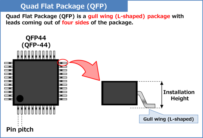
QFP stands for "Quad Flat Package".
Quad Flat Package (QFP) is a gull wing (L-shaped) package with leads coming out of four sides of the package.
The number after QFP indicates the number of pins. For example, QFP44 means a 44-pin QFP.
There are various pin pitches such as 1.0mm, 0.8mm, 0.65mm, 0.5mm, 0.4mm, and 0.3mm. Note that as the pin pitch becomes narrower, the lead pins bend more easily.
In addition, those with gull wing (L-shaped) leads coming out of the two sides of the package are called Small Outline Package (SOP).
There are various types of QFP, such as BQFP and GQFP.
Related article
The following article explains the "Quad Flat Package (QFP)" in detail. If you are interested, please check it out from the link below. 続きを見る
What is Quad Flat Package (QFP)?
Quad Flat J-leaded package (QFJ)
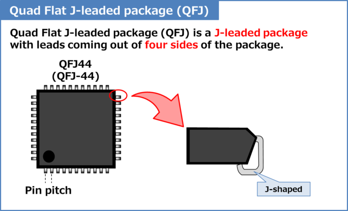
QFJ stands for "Quad Flat J-leaded package".
Quad Flat J-leaded package (QFJ) is a J-leaded package with leads coming out of four sides of the package. The pin pitch of the Quad Flat J-leaded package (QFJ) is 50 mils (1.27mm).
QFJ (Quad Flat J-leaded package) has 18 to 84 pins.
The number after QFJ indicates the number of pins. For example, QFJ44 means a 44-pin QFJ.
Compared to Quad Flat Package (QFP), which has a gull wing (L-shaped) lead shape, Quad Flat J-leaded package (QFJ), which has a J-shaped lead shape, has the advantage of less lead deformation.
In addition, those with J-shaped leads coming out of the two sides of the package are called Small Outline J-leaded package (SOJ).
There are various types of QFJ, such as P-QFJ and C-QFJ.
Related article
The following article explains the "Quad Flat J-leaded package (QFJ)" in detail. If you are interested, please check it out from the link below. 続きを見る
What is Quad Flat J-leaded package (QFJ)?
Quad Flat Non-leaded package (QFN)
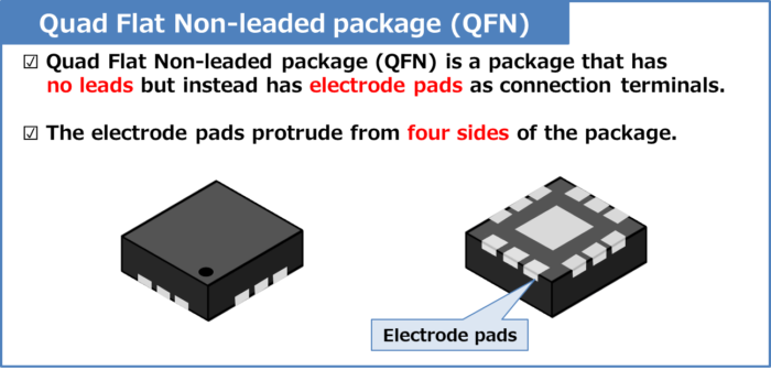
QFN stands for "Quad Flat Non-leaded package".
Quad Flat Non-leaded package (QFN) is a package that has no leads but instead has electrode pads as connection terminals. The electrode pads protrude from four sides of the package.
Since Quad Flat Non-leaded package (QFN) has no leads, the package can be made almost the same size as the chip size.
In addition, those with electrode pads coming out of the two sides of the package are called Small Outline Non-leaded package (SON).
There are various types of QFN, such as LQFN and TQFN.
Related article
The following article explains the "Quad Flat Non-leaded package (QFN)" in detail. If you are interested, please check it out from the link below. 続きを見る
What is Quad Flat Non-leaded package (QFN)?
Quad Flat I-leaded package (QFI)
QFI stands for "Quad Flat I-leaded package".
Quad Flat I-leaded package (QFI) is a I-leaded package with leads coming out of four sides of the package.
In addition, those with I-shaped leads coming out of the two sides of the package are called Small Outline I-leaded package (SOI).
Quad Flat F-leaded package (QFF)
QFF stands for "Quad Flat F-leaded package".
Quad Flat F-leaded package (QFF) is a flat lead package with leads coming out of four sides of the package.
In addition, those with flat leads coming out of the two sides of the package are called Small Outline F-leaded package (SOF).
Pin Grid Array (PGA)
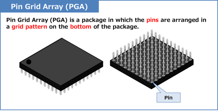
PGA stands for "Pin Grid Array".
Pin Grid Array (PGA) is a package in which the pins are arranged in a grid pattern on the bottom of the package.
Pin Grid Array (PGA) pin pitch is typically 2.54mm (100 mils). Pin Grid Arrays (PGA) may have more than 400 pins.
Until the development of surface-mountable Ball Grid Array (BGA), Pin Grid Array (PGA) was the mainstream high-pin-count package for CPUs and other components used in PCs.
There are various types of PGA, such as SPGA and IPGA.
Related article
The following article explains the "Pin Grid Array (PGA)" in detail. If you are interested, please check it out from the link below. 続きを見る
What is Pin Grid Array (PGA)?
Land Grid Array (LGA)
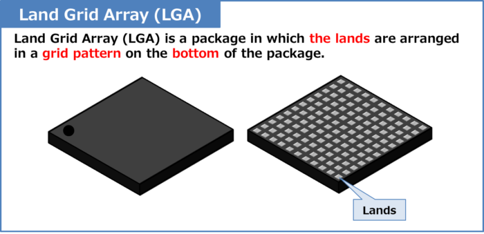
LGA stands for "Land Grid Array".
Land Grid Array (LGA) is a package in which the lands are arranged in a grid pattern on the bottom of the package.
Unlike Ball Grid Array (BGA), Land Grid Array (LGA) can be mounted using sockets. There are special sockets that are mounted by pressing against a kenzan-shaped electrode. Also, since the terminals of Land Grid Array (LGA) are lands, the mounting height can be reduced compared to that of Ball Grid Array (BGA).
There are various types of LGA, such as FLGA and ILGA.
Related article
The following article explains the "Land Grid Array (LGA)" in detail. If you are interested, please check it out from the link below. 続きを見る
What is Land Grid Array (LGA)?
Ball Grid Array (BGA)
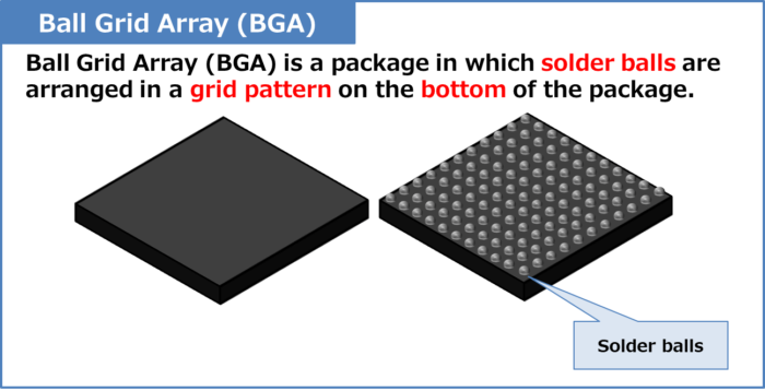
BGA stands for "Ball Grid Array".
Ball Grid Array (BGA) is a package in which the solder balls are arranged in a grid pattern on the bottom of the package.
There are various pin pitches such as 1.27mm, 1.0mm, 0.8mm, 0.75mm, 0.65mm, 0.5mm,and 0.4mm.
There are various types of BGA, such as FBGA and IBGA.
Related article
The following article explains the "Ball Grid Array (BGA)" in detail. If you are interested, please check it out from the link below. 続きを見る
What is Ball Grid Array (BGA)?
Other Packages
下記のパッケージを説明しました。
Types of IC Package
- Insertion mount package
- SIP,ZIP,DIP
- Surface mount package with leads coming out of two sides
- SOP,SOJ,SON,SOI,SOF(Only SON is non-lead)
- Surface mount package with leads coming out of four sides
- QFP,QFJ,QFN,QFI,QFF(Only QFN is non-lead)
- Packages with terminals arranged in a grid pattern from the bottom of the package
- PGA,BGA,LGA
From now on, we will describe the packages other than those listed above.
IC Package with Tape
Dual Tape carrier Package (DTP)
DTP stands for "Dual Tape carrier Package".
Dual Tape carrier Package (DTP) is the tape-structured package with leads coming out of two sides of the package.
Tape Automated Bonding is used to bond IC chips and TAB tape on which semiconductor integrated circuits are mounted. Packages using this method are also called Tape Carrier Package (TCP).
Quad Tape carrier Package (QTP)
QTP stands for "Quad Tape carrier Package".
Quad Tape carrier Package (QTP) is the tape-structured package with leads coming out of four sides of the package.
IC Package containing the name CSP
Chip Size Package/Chip Scale Package (CSP)
CSP stands for "Chip Size Package/Chip Scale Package".
Chip Scale Package (CSP) is a package that is much smaller than Ball Grid Array (BGA) and has external dimensions close to those of the semiconductor chip to be mounted.
There is no JEITA name for this type of package because it indicates its characteristics rather than its external shape.
Wafer Lebel CSP (WL-CSP)
WL-CSP stands for "Wafer Lebel CSP".
WL-CSP is a CSP manufactured by rewiring, sealing, and external terminaling in wafer state, and finally separating and individualizing the wafers
Other IC Package
Leadless Leadframe Package (LLP)
LLP stands for "Leadless Leadframe Package".
LLP is a type of CSP package that uses a leadframe.
It is an ultra-small and ultra-thin package, smaller than TSSOP. It was developed by National Semiconductor Corporation, and the name LLP is a registered trademark.
Dual Flatpack No-leaded (DFN)
DFN stands for "Dual Flatpack No-leaded".
DFN has electrode pads on two or four sides of the package. DFN with electrode pads on one side are also available, but those with electrode pads on two or four sides are generally used. 4-sided DFN are also called Quad Flat Non-leaded package (QFN).
Leadless Leadframe Package (LLP) and Dual Flatpack No-leaded (DFN) are similar in structure. In Leadless Leadframe Package (LLP), the terminal pad is embedded in the package, whereas in Dual Flatpack No-leaded (DFN), a plate terminal pulled out from the side of the package is bent inward to form an electrode pad.
Multi Chip Package (MCM)
MCM stands for "Multi Chip Module".
Multi Chip Package (MCM) is a module that contains multiple semiconductor chips and elements in a single package or module.
System in a Package (SiP)
SIP stands for "System in a Package".
System in a Package (SiP) is a module that contains multiple semiconductor chips in a single package. The counterpart term is "System-On-a-Chip (SOC)".
Multi Chip Package (MCM) is also a module that encapsulates multiple chips in a single package, but System in a Package (SiP) is characterized by the fact that it has some system functions in its package.
Package on a Package (PoP)
PoP stands for "Package on a Package".
Package on a Package (PoP) is a technology to stack packages on top of packages. It enables high functionality in a small mounting area.
Package in a Package (PiP)
PiP stands for "Package in a Package".
Package in a Package (PiP) is a technology that encapsulates the package inside the package.
Quad In-line Package (QIP / QUIP)
QIP / QUIP stands for "Quad In-line Package".
Quad In-line Package (QIP / QUIP) is a package with alternating Dual In-line Package (DIP) legs.
A SIP with alternating legs is called a Zig-zag In-line Package (ZIP).
Thin Small Outline Circuit (TSOC)
TSOC stands for "Thin Small Outline Circuit".
Thin Small Outline Circuit (TSOC) is a low-pin count version of Small Outline J-leaded package (SOJ).
The pin pitch is 1.27mm, the same as Small Outline J-leaded package (SOJ), but the body size is smaller.
Ceramic Flat Package (CFP)
CFP stands for "Ceramic Flat Package".
Ceramic Flat Package (CFP) is a thin ceramic package. Structurally, it is similar to a thinner Ceramic Dual In-line Package (C-DIP).
Since it was developed at a time when surface mounting was not very popular, it can be inserted and mounted by bending the pins.
Lead Less Chip Carrier (LLCC)
LLCC stands for "Lead Less Chip Carrier".
Lead Less Chip Carrier (LLCC) is a package with electrode pads on the ceramic surface and no lead wires.
Lead Less Chip Carrier (LLCC) is sometimes also called Quad Flat Non-leaded package (QFN).
Fan Out Wafer Level Package (FOWLP)
FOWLP stands for "Fan Out Wafer Level Package".
Fan Out Wafer Level Package (FOWLP) is a package with external pins in an area larger than the semiconductor chip to support multiple pins.
The area of the package is larger than that of the semiconductor chip, and by extending the external pins to an area larger than the semiconductor chip, more input/output pins are secured.
Compared to Ball Grid Array (BGA), thinner and shorter wiring lengths are possible.
Chip On Board (COB)
COB stands for "Chip On Board".
Chip On Board (COB) is a technology for mounting chips on substrates.
In Chip On Board (COB), chips are mounted on the substrate with resin, and the circuit pattern and chip electrodes are connected with pure gold wires. Compared to surface mounting of packaged products, Chip On Board (COB) enables a reduction in mounting area and a thinner profile.
Chip On Film (COF)
COF stands for "Chip On Film".
Chip On Film (COF) is a technology to mount chips on flexible substrates.
While the mounting target of Chip On Board (COB) was a substrate, the mounting target of Chip On Film (COF) is a thin and flexible flexible flexible substrate (polyimide film substrate).
Chip On Glass (COG)
COG stands for "Chip On Glass".
Chip On Glass (COG) is a technology to mount chips on glass substrates.
While the mounting target of Chip On Board (COB) was a substrate, the mounting target of Chip On Glass (COG) is a glass substrates.
Compared to Chip On Board (COB), Chip On Glass (COG) is more compact, but passive components cannot be mounted on glass substrates, so they must be mounted externally.
Surface Vertical Package (SVP)
SVP stands for "Surface Vertical Package".
Surface Vertical Package (SVP) is a package with leads coming out of one side of the package, the leads are V-shaped, and the package is designed for insertion mounting.
Summary
In this article, the following information on the "Types of semiconductor (IC and transistor) packages" was explained.
Thank you for reading.