There are various types of semiconductor and IC packages, such as Ball Grid Array (BGA) and Pin Grid Array (PGA).
Regarding the "Ball Grid Array (BGA)", this article will explain the information below.
- Ball Grid Array (BGA) Definition
- Types of Ball Grid Array (BGA)
Ball Grid Array (BGA) Definition
BGA stands for "Ball Grid Array".
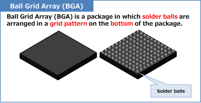
Ball Grid Array (BGA) is a package in which the solder balls are arranged in a grid pattern on the bottom of the package.
There are various pin pitches such as 1.27mm, 1.0mm, 0.8mm, 0.75mm, 0.65mm, 0.5mm,and 0.4mm.
The "package mounting height", "pin pitch", etc. change depending on the English letter in front of the BGA.
For example, "L" means that the package installation height L is "1.20mm < L ≤ 1.70mm". Therefore, "LBGA" with "L" in front of BGA means BGA with a package installation height of "1.20mm < L ≤ 1.70mm".
Ball Grid Array (BGA) has the following advantages and disadvantages compared to QFP (Quad Flat Package).
Advantages
- Since there is no risk of lead deformation, mounting defects on printed circuit boards are less likely to occur and mounting work can be performed more efficiently.
- Since there are no leads protruding from the package, the package can be miniaturized. In other words, mounting density can be increased.
- Terminals can be arranged in high density.
- Suitable for high-speed LSI packages because the lead inductance is small.
Disadvantages
- Once soldering is done, it is difficult to repair because the internal condition cannot be determined.
- The state of soldering cannot be inspected from the outside.
- Manual soldering is not possible, so soldering must be done in a reflow oven.
- The board must be reheated when removing components, and depending on the heat resistance temperature of the components mounted in the back-end process of the BGA package, it may not be repairable.
- Since the thermal expansion coefficient of the package is different from that of the substrate, in the case of BGA packages that generate heat while energized, repeated thermal expansion and contraction may distort the package or substrate, causing cracks at the soldering contacts and resulting in a broken wire condition.
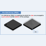
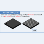
Difference between "PGA", "LGA", and "BGA"
The package name changes depending on whether the grid array on the bottom of the package is pins, lands, or solder balls.
- Pins: Pin Grid Array (PGA)
- Lands: Land Grid Array (LGA)
- Solder balls: Ball Grid Array (BGA)
The following article explains "Pin Grid Array (PGA)" and "Land Grid Array (LGA)" in detail. If you are interested, please check it out from the link below.
-

What is Pin Grid Array (PGA)?
続きを見る
-
What is Land Grid Array (LGA)?
続きを見る
Types of Ball Grid Array (BGA)
FBGA
The "F" in front of BGA stands for "Fine pitch".
The "F" makes the pin pitch shorter as shown below.
About Pin Pitch
- When the basic package is BGA or LGA (FBGA or FLGA)
- Pin pitch is 0.8 mm or less
- When the basic package is QFP (FQFP)
- Pin pitch is 0.5 mm or less
Therefore, "Fine-pitch Ball Grid Array (FBGA)" means BGA with a pin pitch of 0.8 mm or less.
IBGA
The "I" in front of BGA stands for "Interstitial.
Therefore, "Interstitial Ball Grid Array (IBGA)" means BGA with package terminals that are not grid-shaped (e.g., staggered pattern).
LBGA
The "L" in front of BGA means that the package installation height L is "1.20mm < L ≤ 1.70mm".
Therefore, "Low-Profile Ball Grid Array (LBGA)" is a BGA with a package installation height of "1.20mm < L ≤ 1.70mm".
LFBGA
The "L" in front of FBGA means that the package installation height L is "1.20mm < L ≤ 1.70mm".
Therefore, "Low-Profile Fine-pitch Ball Grid Array (LFBGA)" is a FBGA with a package installation height of "1.20mm < L ≤ 1.70mm".
TBGA
The "T" in front of BGA means that the package installation height T is "1.00mm < T ≤ 1.20mm".
Therefore, "Thin Ball Grid Array (TBGA)" is a BGA with a package installation height of "1.00mm < T ≤ 1.20mm".
TFBGA
The "T" in front of FBGA means that the package installation height T is "1.00mm < T ≤ 1.20mm".
Therefore, "Thin Fine-pitch Ball Grid Array (TFBGA)" is a FBGA with a package installation height of "1.00mm < T ≤ 1.20mm".
VBGA
The "V" in front of BGA means that the package installation height V is "0.80mm < V ≤ 1.00mm".
Therefore, "Very thin Ball Grid Array (VBGA)" is a BGA with a package installation height of "0.80mm < V ≤ 1.00mm".
VFBGA
The "V" in front of FBGA means that the package installation height V is "0.80mm < V ≤ 1.00mm".
Therefore, "Very thin Fine-pitch Ball Grid Array (VFBGA)" is a FBGA with a package installation height of "0.80mm < V ≤ 1.00mm".
WBGA
The "W" in front of BGA means that the package installation height W is "0.65mm < W ≤ 0.80mm".
Therefore, "Very-Very thin Ball Grid Array (WBGA)" is a BGA with a package installation height of "0.65mm < W ≤ 0.80mm".
WFBGA
The "W" in front of FBGA means that the package installation height W is "0.65mm < W ≤ 0.80mm".
Therefore, "Very-Very thin Fine-pitch Ball Grid Array (WFBGA)" is a FBGA with a package installation height of "0.65mm < W ≤ 0.80mm".
UBGA
The "U" in front of BGA means that the package installation height U is "0.50mm < U ≤ 0.65mm".
Therefore, "Ultra-thin Ball Grid Array (UBGA)" is a BGA with a package installation height of "0.50mm < U ≤ 0.65mm"
UFBGA
The "U" in front of FBGA means that the package installation height U is "0.50mm < U ≤ 0.65mm".
Therefore, "Ultra-thin Fine-pitch Ball Grid Array (UFBGA)" is a FBGA with a package installation height of "0.50mm < U ≤ 0.65mm"
XBGA
The "X" in front of BGA means that the package installation height X is "X ≤ 0.50mm".
Therefore, "Extra thin Ball Grid Array (XBGA)" is a BGA with a package installation height of "X ≤ 0.50mm"
XFBGA
The "X" in front of FBGA means that the package installation height X is "X ≤ 0.50mm".
Therefore, "Extra thin Fine-pitch Ball Grid Array (XFBGA)" is a FBGA with a package installation height of "X ≤ 0.50mm"
HBGA
The "H" in front of BGA stands for "Heat sink".
Therefore, "HBGA" means a "BGA with Heat sink". A heat-dissipating surface called a thermal pad is provided on the board mounting side surface.
HLBGA
The "H" in front of LBGA stands for "Heat sink".
Therefore, "HLBGA" means a "LBGA with Heat sink". A heat-dissipating surface called a thermal pad is provided on the board mounting side surface.
HTBGA
The "H" in front of TBGA stands for "Heat sink".
Therefore, "HTBGA" means a "TBGA with Heat sink". A heat-dissipating surface called a thermal pad is provided on the board mounting side surface.
HVBGA
The "H" in front of VBGA stands for "Heat sink".
Therefore, "HVBGA" means a "VBGA with Heat sink". A heat-dissipating surface called a thermal pad is provided on the board mounting side surface.
HWBGA
The "H" in front of WBGA stands for "Heat sink".
Therefore, "HWBGA" means a "WBGA with Heat sink". A heat-dissipating surface called a thermal pad is provided on the board mounting side surface.
HUBGA
The "H" in front of UBGA stands for "Heat sink".
Therefore, "HUBGA" means a "UBGA with Heat sink". A heat-dissipating surface called a thermal pad is provided on the board mounting side surface.
HXBGA
The "H" in front of XBGA stands for "Heat sink".
Therefore, "HXBGA" means a "XBGA with Heat sink". A heat-dissipating surface called a thermal pad is provided on the board mounting side surface.
P-BGA
The "P-" in front of BGA stands for "Plastic".
Therefore, "Plastic BGA (P-BGA)" means a "BGA whose package material is plastic".
C-BGA
The "C-" in front of BGA stands for "Ceramic".
Therefore, "Ceramic BGA (C-BGA)" means a "BGA whose package material is ceramic".
S-BGA
The "S-" in front of BGA stands for "Silicon".
Therefore, "S-BGA (Silicon BGA)" means a "BGA whose package material is silicon".
Other
- Enhanced BGA (EBGA)
- Flex Tape BGA (FTBGA)
- PFBGA
- FBGA with terminal for stack
- PLFBGA
- LFBGA with terminal for stack
- PTFBGA
- TFBGA with terminal for stack
- PVFBGA
- VFBGA with terminal for stack
- PWFBGA
- WFBGA with terminal for stack
- PUFBGA
- UFBGA with terminal for stack
- PXFBGA
- XFBGA with terminal for stack
- Flip Chip BGA (FC-BGA)
- A common name for a BGA in which semiconductor chips are connected to the package substrate via face-down connection pumps.
- Multi-Chip FBGA (MC-FBGA)
- Micro SMD
- A small BGA package manufactured by National Semiconductor, available in 4-pin to 42-pin types.
Summary
In this article, the following information on the "Ball Grid Array (BGA)" was explained.
- Ball Grid Array (BGA) Definition
- Types of Ball Grid Array (BGA)
Thank you for reading.
Related article
The packages of semiconductors (IC and transistor) other than "Ball Grid Array (BGA)" described in this article are explained in detail in the following article. If you are interested, please check it out from the link below.
- Types of IC Packages
- What is Small Outline Transistor (SOT)?
- What is Small Outline Diode (SOD)?
- What is Transistor Outline (TO)?
- What is Single In-line Package (SIP)?
- What is Dual In-line Package (DIP)?
- What is Zig-zag In-line Package (ZIP)?
- What is Small Outline Package (SOP)?
- What is Small Outline Non-leaded package (SON)?
- What is Small Outline J-leaded package (SOJ)?
- What is Quad Flat Package (QFP)?
- What is Quad Flat Non-leaded package (QFN)?
- What is Quad Flat J-leaded package (QFJ)?
- What is Land Grid Array (LGA)?
- What is Pin Grid Array (PGA)?