A flyback converter is one way to convert a DC voltage while keeping the input and output electrically isolated.
This article uses circuit diagrams and waveforms to explain the following topics.
- What a flyback converter is
- How a flyback converter differs from a buck-boost converter
- How a flyback converter works, its operating modes, its equations, and its simulation results
What Is a Flyback Converter?
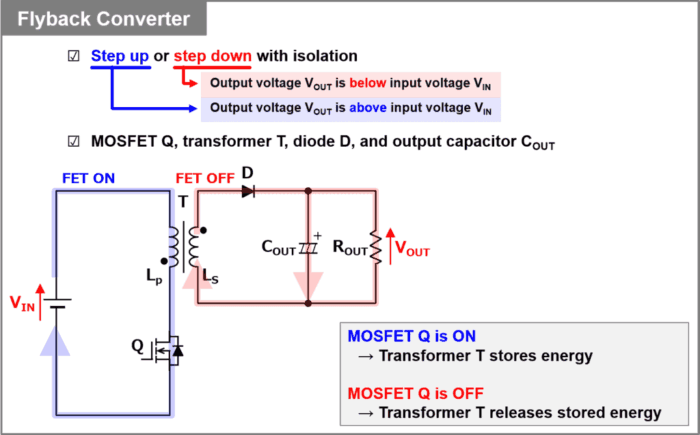
A flyback converter is an isolated converter that can step voltage up or down.
Isolated converters come in several types, including flyback converters and forward converters. Compared with other isolated converters, the flyback converter uses fewer components. It consists of a MOSFET \(Q\), a transformer \(T\), a diode \(D\), and an output capacitor \(C_{OUT}\). The primary and secondary windings of transformer \(T\) are connected with opposite polarities.
We will look at the operating principle in more detail below. While MOSFET \(Q\) is on, transformer \(T\) stores energy. When MOSFET \(Q\) turns off, the transformer releases that energy through its secondary winding. Diode \(D\) rectifies the output, and output capacitor \(C_{OUT}\) smooths it to produce a DC voltage.
The flyback converter has the following advantages and disadvantages.
Advantages
- It uses fewer components than other isolated converters.
- It can step voltage up or down.
- Transformer \(T\) provides electrical isolation between the primary and secondary sides.
Disadvantages
- The output capacitor carries a high ripple current.
- The flyback converter uses a capacitor-input output stage without a smoothing inductor on the secondary side. As a result, the capacitor carries a high ripple current, making the circuit poorly suited to high-current applications.
- MOSFET \(Q\) and diode \(D\) carry high peak currents.
Other switching devices, such as a bipolar junction transistor, can be used in place of MOSFET \(Q\).
Flyback and Buck-Boost Converter Circuits and Their Differences
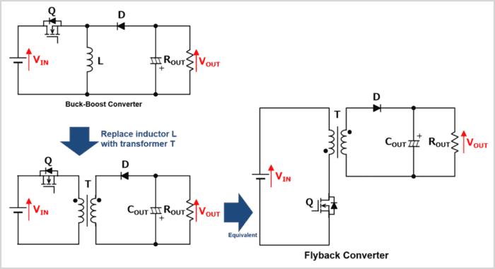
Replacing inductor \(L\) in a buck-boost converter with transformer \(T\) gives an equivalent flyback converter circuit. The magnetizing inductance of transformer \(T\) takes the place of inductor \(L\).
In a buck-boost converter, the input and output voltages have opposite polarities. In a flyback converter, connecting the primary and secondary windings of transformer \(T\) with opposite polarities allows the input and output voltages to have the same polarity.
How a Flyback Converter Works
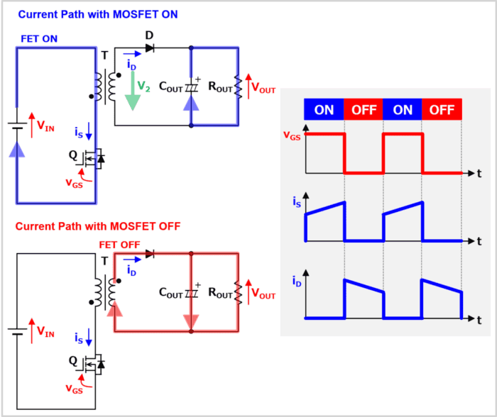
Let’s look at how the flyback converter works with MOSFET \(Q\) on and with it off.
When MOSFET \(Q\) Is On
When MOSFET \(Q\) is on, current flows from the input supply \(V_{IN}\) through the primary winding of transformer \(T\) and then through MOSFET \(Q\). This current stores energy in transformer \(T\).
An electromotive force \(V_2\) is induced in the secondary winding of transformer \(T\) during this interval. The diode blocks current from the secondary winding of transformer \(T\) to the load. During this interval, output capacitor \(C_{OUT}\) discharges and supplies current to load resistor \(R_{OUT}\).
When MOSFET \(Q\) Is Off
When MOSFET \(Q\) turns off, the energy stored in transformer \(T\) is released through the secondary winding and delivered to the output through diode \(D\).
The current path runs from the secondary winding of transformer \(T\), through diode \(D\), to the output stage (output capacitor \(C_{OUT}\) and load resistor \(R_{OUT}\)). While diode current \(D\) exceeds the current through load resistor \(R_{OUT}\), current flows to load resistor \(R_{OUT}\), and the excess current charges output capacitor \(C_{OUT}\).
When diode current \(i_D\) drops below the current through load resistor \(R_{OUT}\), output capacitor \(C_{OUT}\) supplies the difference.
Flyback Converter Operating Modes
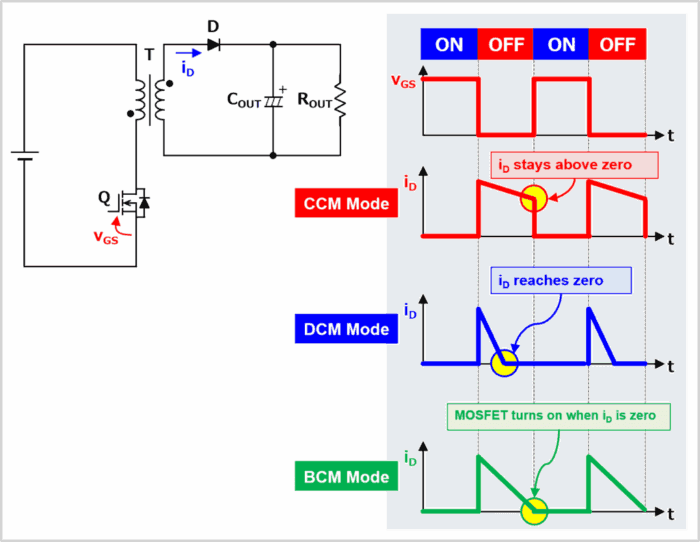
The flyback converter has three operating modes, distinguished by the waveform of diode current \(i_D\) while MOSFET \(Q\) is off.
- CCM (continuous conduction mode)
- Diode current \(i_D\) continues to flow throughout the interval when MOSFET \(Q\) is off and stays above zero.
- DCM (discontinuous conduction mode)
- Diode current \(i_D\) reaches zero while MOSFET \(Q\) is off, leaving an interval with zero current.
- BCM (boundary conduction mode)
- When diode current \(i_D\) reaches zero while MOSFET \(Q\) is off, MOSFET \(Q\) turns on.
- BCM is the boundary between CCM and DCM.
Let’s look at each operating mode in more detail.
CCM
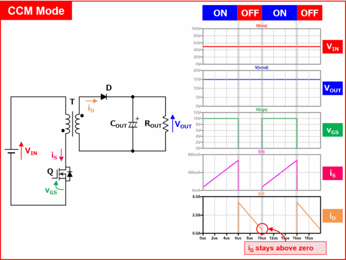
In CCM, diode current \(i_D\) continues to flow and stays above zero throughout the interval when MOSFET \(Q\) is off. CCM stands for continuous conduction mode or continuous current mode.
CCM has the following advantages and disadvantages.
Advantages
Lower current ripple offers the following benefits.
- The peak currents on the primary and secondary sides are lower.
- The required capacitance can be reduced.
- Input and output ripple voltages can be reduced.
Disadvantages
- MOSFET \(Q\) turns on while diode \(D\) is still conducting. This causes a reverse recovery current to flow through diode \(D\), resulting in reverse recovery loss.
- When MOSFET \(Q\) turns on, the current \(i_S\) through \(Q\) is above 0 A, which increases switching loss.
- The primary-side inductance must be higher, which makes transformer \(T\) larger.
DCM
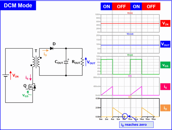
In DCM, diode current \(i_D\) reaches zero while MOSFET \(Q\) is off, leaving an interval with zero current. DCM stands for discontinuous conduction mode or discontinuous current mode.
DCM has the following advantages and disadvantages.
Advantages
- MOSFET \(Q\) turns on when the current through diode \(D\) is zero, so diode \(D\) carries no reverse recovery current.
- When MOSFET \(Q\) turns on, the current \(i_S\) through \(Q\) rises from 0 A, so switching loss is lower.
- The primary-side inductance can be lower, allowing for a smaller transformer.
Disadvantages
Higher current ripple leads to the following drawbacks.
- The peak currents on the primary and secondary sides are higher.
- More capacitance is required.
- Input and output ripple voltages are higher.
BCM
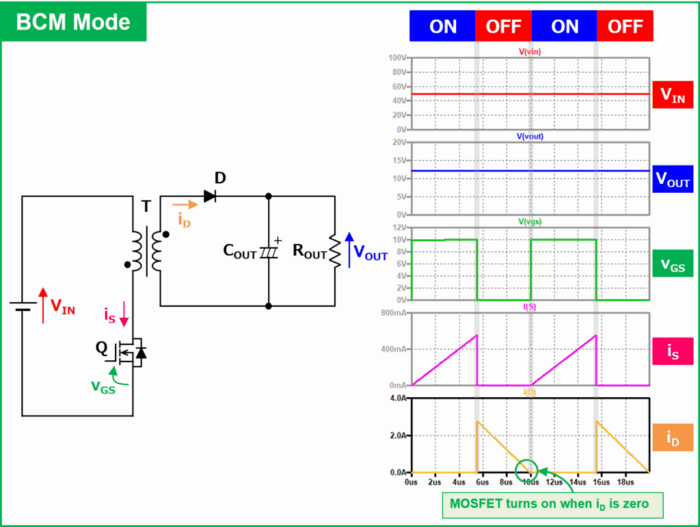
In BCM, MOSFET \(Q\) turns on as soon as diode current \(i_D\) reaches zero while MOSFET \(Q\) is off. BCM stands for boundary conduction mode or boundary current mode.
BCM has the same advantages and disadvantages as DCM, so the DCM discussion also applies here.
Flyback Converter Output Voltage Equations
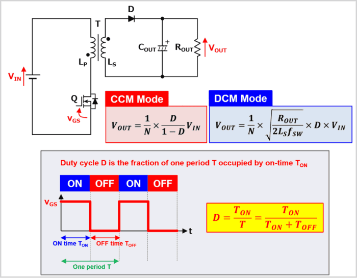
The following equations give the output voltage \(V_{OUT}\) of a flyback converter. The equation for \(V_{OUT}\) differs between CCM and DCM.
In CCM
\begin{eqnarray}
V_{OUT}=\frac{1}{N}×\frac{D}{1-D}V_{IN}\tag{1}
\end{eqnarray}
In DCM
\begin{eqnarray}
V_{OUT}=\frac{1}{N}×\sqrt{\displaystyle\frac{R_{OUT}}{2L_Sf_{SW}}}×D×V_{IN}\tag{2}
\end{eqnarray}
In Equation (2), \(L_S\) is the secondary inductance of transformer \(T\), and \(f_{SW}\) is the switching frequency of MOSFET \(Q\). The duty cycle \(D\) is the fraction of one switching period \(T\) for which MOSFET \(Q\) is on. The on-time is \(T_{ON}\), giving the following expression.
\begin{eqnarray}
D=\frac{T_{ON}}{T}=\frac{T_{ON}}{T_{ON}+T_{OFF}}=T_{ON}×f_{SW}\tag{3}
\end{eqnarray}
Equation (3) shows that the duty cycle \(D\) is less than 1.
In Equations (1) and (2), \(N\) is the turns ratio of transformer \(T\). If \(N_1\) is the number of turns on the primary winding and \(N_2\) is the number on the secondary winding, the turns ratio is given by the following equation.
\begin{eqnarray}
N=\frac{N_1}{N_2}\tag{4}
\end{eqnarray}
Equation (1) is obtained by multiplying the buck-boost converter equation for output voltage \(V_{OUT}\) by \(-\displaystyle\frac{1}{N}\).
Flyback Converter Simulation
CCM Simulation
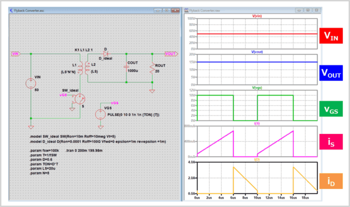
The figure above shows the LTspice simulation results for the flyback converter.
From top to bottom, the waveforms on the right show the following signals.
- Input voltage \(V_{IN}\)
- Output voltage \(V_{OUT}\)
- Drive signal \(v_{GS}\) for switch \(S\)
- Current \(i_S\) through switch \(S\)
- Current \(i_D\) through diode \(D\)
To ignore losses in MOSFET \(Q\) and diode \(D\), the simulation uses an ideal switch in place of MOSFET \(Q\) and an ideal diode in place of diode \(D\).
The input voltage \(V_{IN}\) is 50 V, the duty cycle \(D\) of ideal switch \(S\) is 0.6, and the turns ratio \(N\) is 5. Substituting these values into Equation (1) gives the output voltage \(V_{OUT}\).
\begin{eqnarray}
V_{OUT}=\frac{1}{N}×\frac{D}{1-D}V_{IN}=\frac{1}{5}×\frac{0.6}{1-0.6}×50=15{\mathrm{[V]}}
\end{eqnarray}
The simulation also shows that the output voltage \(V_{OUT}\) is 15 V. The diode current \(i_D\) is still flowing just before the switch turns on again.
DCM Simulation
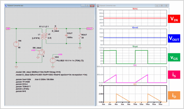
Next, let’s look at the simulation results when the duty cycle \(D\) is reduced so that the converter operates in DCM.
The input voltage \(V_{IN}\) is 50 V, the duty cycle \(D\) of ideal switch \(S\) is 0.4, and the turns ratio \(N\) is 5. The secondary inductance \(L_S\) of transformer \(T\) is 20 μH, the switching frequency \(f_{SW}\) of MOSFET \(Q\) is 100 kHz, and the load resistance \(R_{OUT}\) is 20 Ω.
Using Equation (2), the output voltage \(V_{OUT}\) is calculated as follows.
\begin{eqnarray}
V_{OUT}&=&\frac{1}{N}×\sqrt{\displaystyle\frac{R_{OUT}}{2L_Sf_{SW}}}×D×V_{IN}\\
\\
&=&\frac{1}{5}×\sqrt{\displaystyle\frac{20}{2×20×10^{-6}×100×10^3}}×0.4×50\\
\\
&{\;}{\approx}{\;}&8.94{\mathrm{[V]}}
\end{eqnarray}
The simulation also shows that the output voltage \(V_{OUT}\) is close to 8.94 V. The diode current \(i_D\) reaches zero partway through the off interval and remains at zero until the switch turns on again.
Summary
This article covered the following topics.
- What a flyback converter is
- How a flyback converter works, its operating modes, its equations, and its simulation results
Thank you for reading.